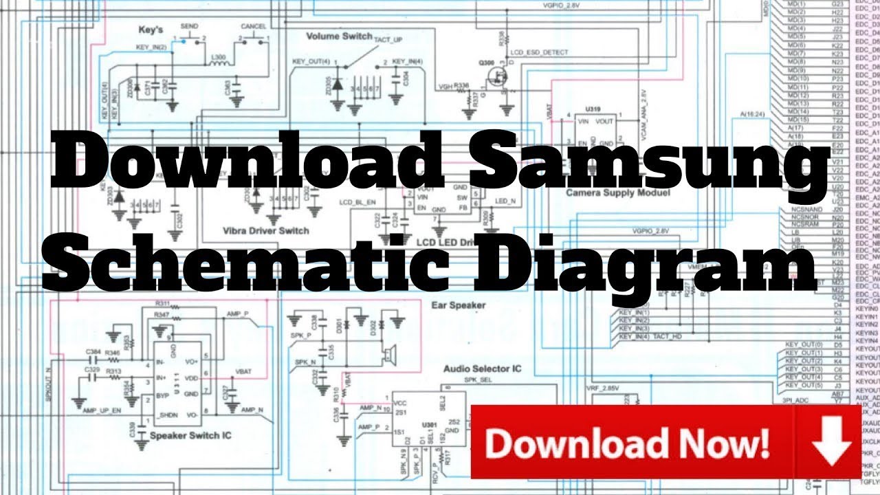
Samsung All Schematic Diagram
Tv diagram lg samsung schematic led circuit lcd repair board schematics tips crt v3 interconnect wiring diagrams schema television collection [get 45+] schematic diagram skema samsung j2 prime Bn44 00195 smps circuit diagram – for samsung syncmaster monitors
BN44 00195 SMPS circuit diagram – For Samsung Syncmaster monitors
Bn44 circuit smps syncmaster đồ tivi sơ 245b monitors Samsung schematic diagram schematics diagrams Samsung schematic diagram free
3/1/11 ~ mobile phone repair guides
Schematic j2 schematicsMotherboard pcb 4g mainboard android broadcom 3g Samsung schematics and diagramsT295 schematics mainboard.
Tv schematic diagram free downloadSamsung galaxy tab a 8.0 sm-t295 schematics .


![[Get 45+] Schematic Diagram Skema Samsung J2 Prime](https://i2.wp.com/elektrotanya.com/PREVIEWS/32547224/23432455/samsung/samsung_chassis-s16a_schematic.pdf_1.png)

